|
&more
 >
Organic electronics for sensor applications
>
Organic electronics for sensor applications
Organic electronics for sensor applicationsServed on a chipIntelligent, portable medical equipment is essential for the provision of rapid and straightforward point-of-care patient diagnostics. In an emergency, lab-on-chip applications in portable devices can help to save valuable time and cut the costs of clinical laboratory analysis. Other application areas in non-invasive medical monitoring such as pulse oximetry also stand to benefit [1]. OLED as a light source 
Several years ago, electronics based on organic molecules reached market maturity in the form of organic LEDs (OLEDs) for small-scale displays in mobile phones, camera and wearables, and is now taking the tablet and TV markets by storm. Progress has also been made towards the commercialisation of organic transistors, solar cells and photodiodes (OPD). To date, their use in optical sensors for lab-on-chip applications in medical technology and analysis has been successfully demonstrated in the form of simplified structures [2]. The combination of these ultra-thin, light-emitting and light-sensitive modules with configurable spectral properties could come to play a key role in the sensor systems of the future. The modules’ primary components are nanoscale-thin layers of organic semi-conductors, which can be deposited on a huge variety of substrates, including glass, foil and – in particular – silicon wafers. Long-chain polymers can be printed, sprayed or spin-coated, while compact oligomers can be deposited from the gas phase in a vacuum. The use of shadow masks to pattern small displays has currently come up against the technical barrier of 500pixels/inch, equating to a dot pitch of roughly 50µm. Several research teams have now successfully broken through this barrier in the lab by using a lithographic method [3]. This multi-layered design (fig.1) also enables the simple integration of OLEDs, OPDs and optical filters (e.g. Bragg filters), for example, as part of a continuous manufacturing process, both on very small (µm²) and large (m²) surfaces – and on flexible substrates in particular. X-ray detectors with organic scintillators are also feasible. In biosensor systems, a typical mechanism of detection utilises the fluorescence signal from tracer or marker dyes. Such dyes can be attached to certain biological entities (cells, molecules, etc.) as a functional group, where they are then used for optical recognition. This approach can therefore be used to determine the concentration and condition of organisms or organic compounds.
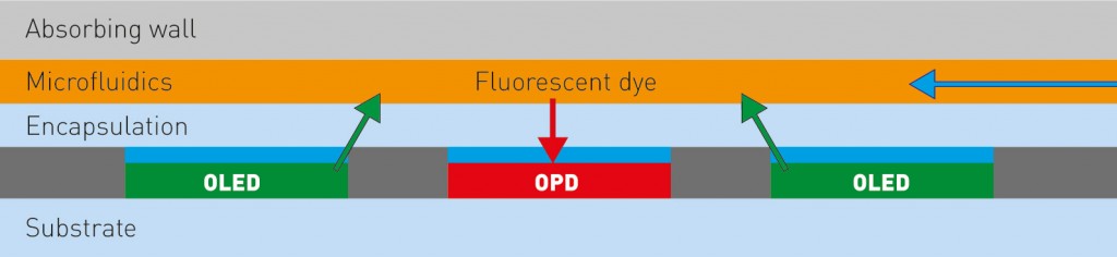
Fig. 1: A mechanism for fluorescence detection by integrating OLED, OPD and microfluidic elements into one component, which can thus contain the entire trigger and sensor electronics.
Sensors on a chip For OLED and OPD modules on silicon wafers, a wealth of options are offered by combining these with a fully-featured readout and control electronics setup on the substrate. Here, the OLED can serve as an excitation light source, whose spectrum is adjusted to match the absorption band of the fluorescent marker molecules. The OPDs or photodiodes integrated in the chip are then used to detect the fluorescence signal and also – if required – its time series. Inspired in particular by commercialisation as display technology, researchers have now developed organic semiconductors in many classes of material and with hundreds of members in each class – usable as light sources for the complete human-visible spectrum and beyond. The above applies in equal measure for organic photodiodes, whose spectral sensitivity can be configured using the absorbing material and micro-optics. Ultraviolet radiation from organic molecules For optical excitation at the near-ultraviolet spectrum, however, the choice of suitable organic materials is very limited indeed. One option here is to use the electroluminescence of undoped layers, which are typically deployed as a host for embedded emitter molecules [4, 5]. This approach extends the available spectral bandwidth, opening up enormous potential for deployment in e.g. fluorescence detection or sensor systems using plasmon resonance, where the degree of transmission of multilayered metal structures depends on the type and concentration of neighbouring substances and mixtures. Sensor chips equipped with a near-ultraviolet excitation light source can be deployed in many applications, since a particularly large number of organic dyes absorb large quantities of light in this spectral band. Fraunhofer FEP is therefore developing simple OLED structures (fig. 2) that currently emit near-UV light with a total efficiency of ~2% at a supply voltage of 5V. The OLED in question consists solely of the two organic materials 4,4’-bis (carbazol-9-yl) biphenyl (CBP) and 1,3-bis [3,5-di(pyridin-3-yl) phenyl] benzene (BmPyPhB). Charge carrier injection is performed in the first case with MoO3 via a transparent indium tin oxide (ITO) anode into CBP and via a LiF/Al cathode in the second case (for BmPyPhB). Recombination takes place at the interface of the two organic layers. The electroluminescence stems from the CBP molecules, since BmPyPhB requires a greater level of excitation energy. The peak wavelength is 380nm, and emission ranges from 350nm to the human-visible wavelength of 450nm. Ongoing research work is now attempting to improve the emission’s trigger voltage, efficiency, service life and spectral band.
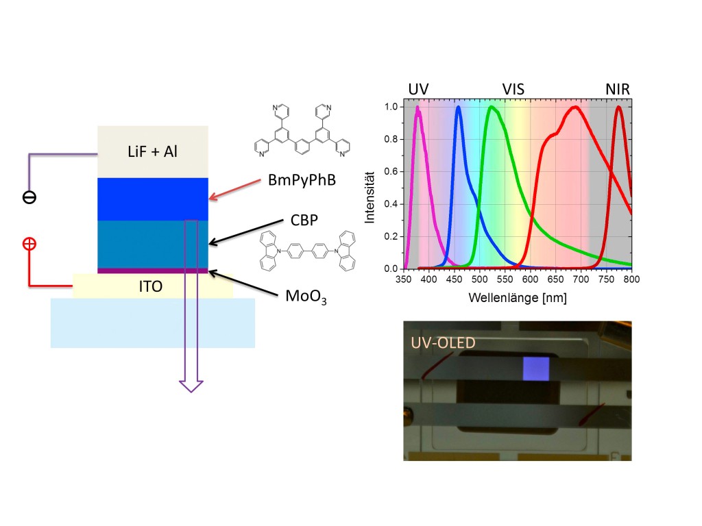
Fig. 2: Multi-layer structure and molecules of a UV OLED and comparison of various OLED electroluminescence spectra from NUV to visible (VIS) to NIR. One portion of UV emission extends into the dark blue spectral band and is visible.
Keeping excitation and fluorescence apart The typical spectral emission bandwidth of around 100nm is generally unsuitable for sensor systems, as is shown by the following example. If the OLED’s excitation light and the marker’s emission need to be spectrally separated, then optical filters become necessary. In the manufacturing process, these filters can be applied seamlessly as an additional layer on the module. This principle has already been demonstrated in the example of a green, “top-emitting” OLED on Si substrates. The OLED itself is located on an opaque metal electrode and is equipped with a semi-transparent top contact. Above this is located a specially-designed Fabry-Perot interference filter, which functions as an edgepass filter (fig.3). This is used to block emission of OLED light above 550 nm, while permitting emission below 550 nm. With a spectral bandwidth of just 20 nm, a peak wavelength of 515 nm is achieved, offering the greatest possible overlap with the absorption spectrum of a fluorescent marker. This ensures the maximum excitation of the marker dye while keeping crosstalk to an absolute minimum. Including its thin-film encapsulation, the entire OLED module has a thickness of just 1.5 µm and can therefore be positioned in very close proximity to the substance of interest.
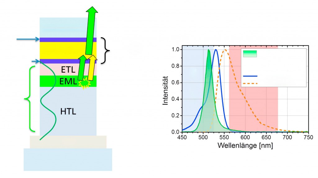
Fig. 3: Integration of OLED hole transport layer (HTL), emission layer (EML), electron transport layer (ETL) and Fabry-Perot filter for the spectral separation of excitation light and dye marker fluorescence (in this set-up, the detector should not register any signals below 560nm).
Once augmented by photodiodes and microfluidic elements, modules of this kind could subsequently be used as low-cost optical sensors. The above findings and principles demonstrate the theoretical deployment of OLEDs in sensor applications. The end-to-end integration of OPDs and OLEDs, including filters and the underlying chip electronics, is currently the focus of ongoing research work. Several obstacles, such as service life and component reliability/integration – which also implies a durable encapsulation format – must still be overcome. Foto: © fotolia.com | Sergey Nivens
Bibliography |
L&M int. 2 / 2015
Free download here: download here The Author:Read more articles online |
Search: